 |
|
Mignonette Assembly Instructions
Below are detailed instructions for the assembly of the game kit. These instructions are designed for the beginner, but even if you are an experienced kit builder, we recommend you take a look before proceeding! |
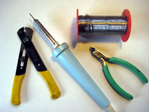 photo 01. |
Step 01: These are the tools you will need:
http://ladyada.net/make/minipov3/make.html Ladyada’s website also has links to some nice tutorials on soldering: http://ladyada.net/learn/soldering/thm.html |
|
| | ||
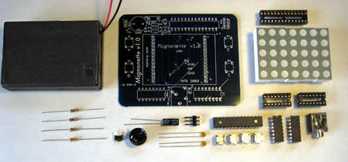 photo 02. |
Step 02: Lay out all of the parts before you. A complete list of parts is available at: mignonette_v1.0-easy-bom.txt You may want to refer to this list as you assemble the kit. All of these parts are available at digikey.com, mouser.com, and jameco.com except for the LED matrix, which is available at bgmicro.com. Suggested parts numbers are given in the parts list. |
|
| | ||
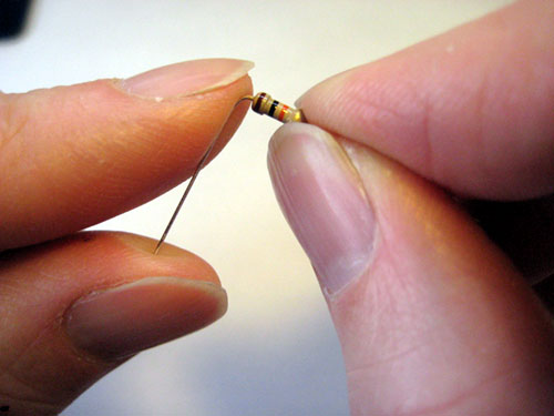 photo 03. |
Step 03: We will start with resistor R1. The colored bands, brown, black, orange, and gold indicate the value of the resistor. (10K Ohms in this case) The wires of all resistors should be bent down on both sides of the part, as shown. Another word for wires that come out of electronic parts is "leads" (pronounced "leeds"). |
|
| | ||
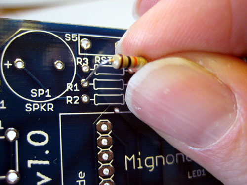 photo 04. |
Step 04: Push the leads from R1 into the pads for R1 on the PCB. "PCB" stands for Printed Circuit Board, and is the blue board that all of the electronic parts are soldered on to. "Pads" are the silver parts on the PCB, usually with a hole in the middle, where the parts will be soldered into. It does not matter which lead of a resistor goes into which pad. This is because resistors are "non-polarized". |
|
| | ||
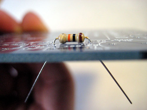 photo 05. |
Step 05: After placing R1 through it’s pads on the PCB, bend its leads outward a little, as shown. This allows the PCB to be turned over without R1 falling out while we solder it in place. |
|
| | ||
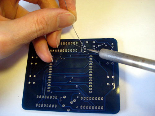 photo 06. |
Step 06: Solder R1. Soldering is done by following these steps:
|
|
| | ||
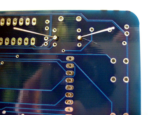 photo 07. |
Step 07: Here you can see R1 soldered into place on the PCB. You can tell a nice solder connection by these three qualities:
|
|
| | ||
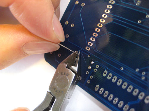 photo 08. |
Step 08: Clip both of the leads of R1 so that they are somewhat flush with the PCB surface. It is not important that the cut be absolutely flush with the PCB. The main thing is that there is not enough of the lead left over to bend over and short out to another pad. IMPORTANT: when clipping leads, always hold the lead with one hand while clipping with the other. This keeps the lead from flying somewhere it is not wanted, such as into your eye, or shorting out some pads somewhere. |
|
| | ||
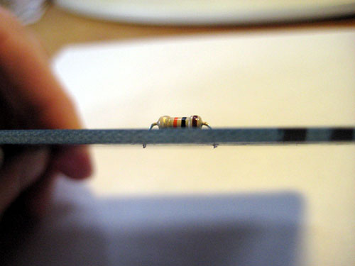 photo 09. |
Step 09: You can see here the leads of R1 clipped to an appropriate length. There is no way they can be bent over to short anything out. |
|
| | ||
 photo 10. |
Step 10: Repeat steps 3 through 9 for the rest of the resistors: R2, R3, and R4. The picture shows where each resistor goes. Refer to the list of parts to find out which colored bands are needed for each resistor. Remember, resistors are non-polarized, so it does not matter which way they go in their pads. |
|
| | ||
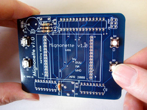 photo 11. |
Step 11: Insert and solder the four game switches into their pads, as shown in the photo. Each switch can be inserted two different ways, and either way is fine. |
|
| | ||
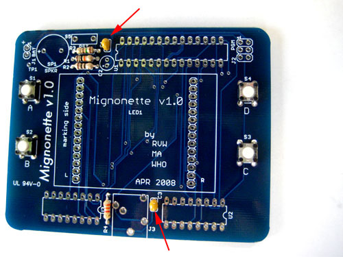 photo 12. |
Step 12: Next we’ll insert and solder capacitors C1 and C3. The leads of these capacitors are already bent correctly. Follow steps 4 through 9 for these two capacitors. These capacitors are non-polarized, so it does not matter which way they are soldered to their pads. |
|
| | ||
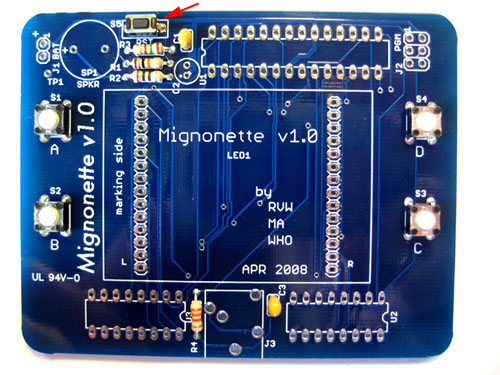 photo 13. |
Step 13: Insert and solder switch S5. It does not matter which way you solder this switch into its pads. |
|
| | ||
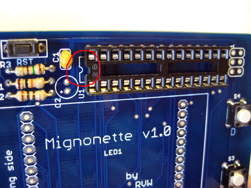 photo 14. |
Step 14: Insert the socket for U1 into its pads. Notice that there is a notch on the white drawing for U1 that matches with the notch on the socket - make sure these line up when you insert it into the PCB. |
|
| | ||
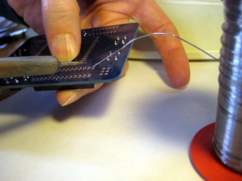 photo 15. |
Step 15: Solder the two opposite corners of the socket into place. Since one hand will be holding the socket and PCB, and the other hand will be holding the solder iron, we do not have a third hand to hold the solder. So, you can use the roll of solder to hold the solder in the correct position, as shown in the photo (bend the solder so that it points down a little bit). If you don’t hold the socket in place when you turn the PCB upside down to solder it, it will fall out. So you will need to hold it onto the PCB with one finger, as shown in the photo. Make sure you don’t touch the metal on the top of the PCB for the pin you are soldering on the bottom (or you will feel the pain!). After soldering one corner of the socket, solder the opposite corner. |
|
| | ||
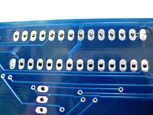 photo 16. |
Step 16: Here you can see two opposite corners of U1 soldered in place. |
|
| | ||
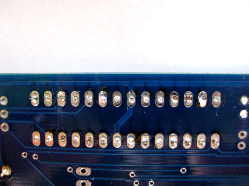 photo 17. |
Step 17: Solder the rest of the 18 pins of U1, so that all 20 pins are soldered. |
|
| | ||
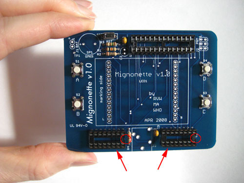 photo 18. |
Step 18: Position U2 onto the PCB as shown in the photo, and solder it in place by repeating steps 14 through 17. Do the same for U3. |
|
| | ||
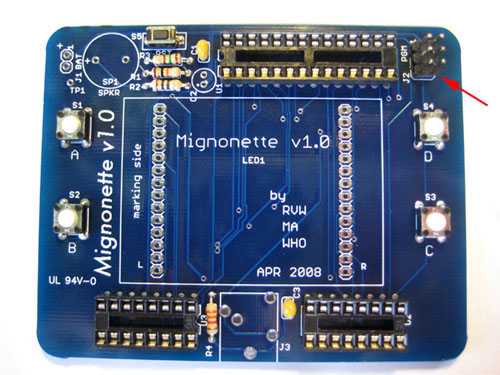 photo 19. |
Step 19: Place the programming connector onto the PCB and solder it in place by repeating steps 15 through 17. J2 can be placed into the PCB in two ways, so make sure the side with the longer pins is facing up. By the way, J2 is the connector that is used to reprogram the game firmware. Pin 1 of this connector is marked on the PCB. |
|
| | ||
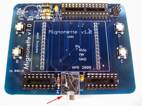 photo 20. |
Step 20: Place J3 onto the PCB as shown in the photo and solder it. |
|
| | ||
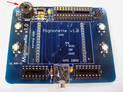 photo 21. |
Step 21: Place the speaker onto the PCB and solder it. The speaker can be placed into the PCB in two ways, and it does not matter which way it is placed. |
|
| | ||
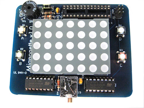 photo 22. |
Step 22: The LED Matrix can be placed into the PCB in two ways, and it does not matter which way it is placed. It may be a little tricky to fit all of 28 pins through the 28 pads, since some of the pins may be a little bit bent. If they are not all lined up, bend the pins a little at a time till they all slide through the 28 pads on the PCB. |
|
| | ||
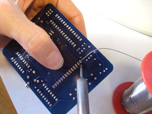 photo 23. |
Step 23: Solder two opposite corners of the LED Matrix into place by following a similar sequence of steps 15 through 17. |
|
| | ||
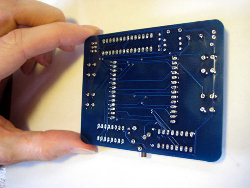 photo 24. |
Step 24: This photo shows all 28 pins of the LED Matrix soldered into place. |
|
| | ||
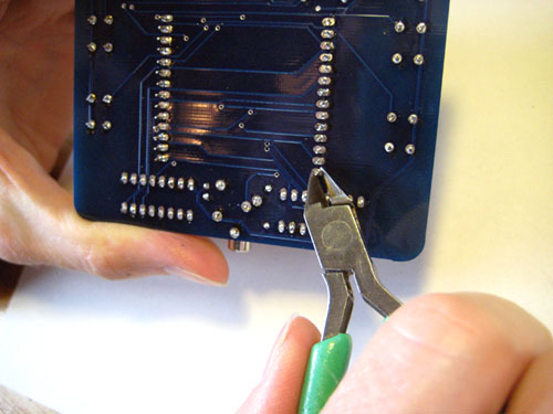 photo 25. |
Step 25: Clip one lead at a time of the LED Matrix. Do all 28 pins. IMPORTANT: remember to hold the lead with one hand as you clip it with the other. You really do not want any of the leads to go into your eye. Also, these small leads can short out pads on the PCB. Be sure to collect the cut leads and keep them away from the PCB. |
|
| | ||
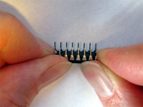 photo 26. |
Step 26: When chips are new, the leads are often bent outward. Ideally, we want the leads of the chips to point straight down, with all leads parallel to each other. By lightly pushing downward on a table you can make all of the leads parallel. Do this for all three chips. "Chip" is another word for Integrated Circuit. |
|
| | ||
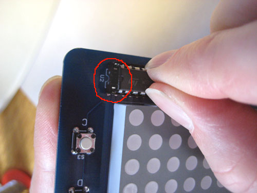 photo 27. |
Step 27: Place chip U2 into it’s socket, making sure that the little notch at one end lines up with the notch in the socket and the PCB. |
|
| | ||
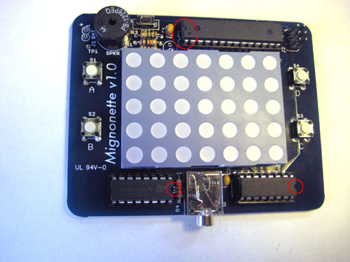 photo 28. |
Step 28: Place chips U1 and U3 into their sockets, making sure all of them have their notches lined up with the notches in the sockets and the PCB, as shown in the photo. |
|
| | ||
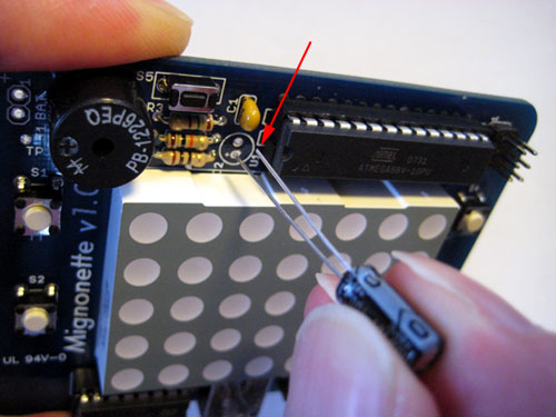 photo 29. |
Step 29: Place capacitor C2 into its pads in the PCB. Capacitor C2 is polarized, meaning it does matter which way you put its two leads in the two pads. The "-" lead is shorter than the "+" lead. The "-" lead is also marked on the side of the capacitor. Make sure you place the part into its pads as shown in the photo. Solder in capacitor C2 and clip its leads. |
|
| | ||
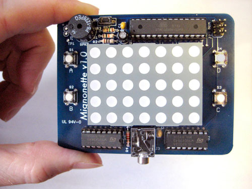 photo 30. |
Step 30: You are now finished soldering in all of the parts into the PCB! This photo shows the end result. |
|
| | ||
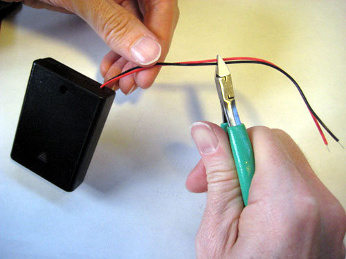 photo 31. |
Step 31: Clip the leads of the battery pack to shorten them. The photo shows about how long to make the wires. The actual length is not critical. |
|
| | ||
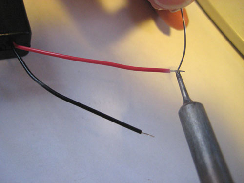 photo 32. |
Step 32: Strip about 1/8" (about 3mm) of insulation off of the end of each lead of the battery pack. Then "tin" the exposed wires. Tinning means melting a thin coat of solder onto a lead. This is done to make it easier to solder it to something else (in this case, the pads on the PCB). |
|
| | ||
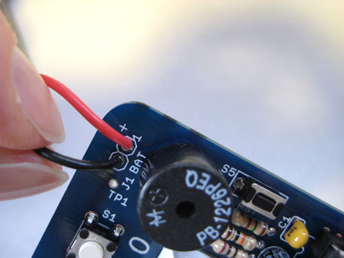 photo 33. |
Step 33: Solder the two wires of the battery pack into its pads in the PCB, as shown in the photo. The convention in electronics is that Red is "+" and Black is "-". |
|
| | ||
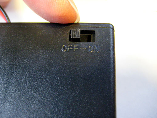 photo 34. |
Step 34: The switch on the battery pack is the On/Off switch for the Mignonette game. For now, turn it to OFF. |
|
| | ||
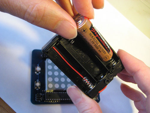 photo 35. |
Step 35: Insert three Alkaline AA batteries into the battery pack. You can turn the Power switch on now, and see what happens. If everything is OK, then you should see the Mignonette light up and make sound. If it does not, turn off the power immediately, and debug. Debugging Suggestions:
|
|
| | ||
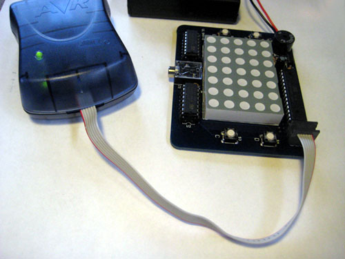 photo 36. |
Step 36: Enjoy! The Mignonette kit comes pre-programmed with a test program and the Munch game. When power is turned ON, the pre-programmed firmware goes into the test program, which lights up each of the LEDs in the 5x7 matrix in red, with a beep on the speaker, then lights up each of the LEDs green, then lights up the middle LED yellow (which is actually blinking very quickly red and green!). Then you can press each of the four buttons to make sure that they each move the lit up LED around the matrix. If all of the LEDs do not light up, or if all of the buttons do not move the LED, then there is a bad solder connection, so try touching them up. To start your Mignonette into the Munch game, hold down the A button while turning the power to ON. You will hear a little start-up tune, followed by three LEDs in the middle of the matrix light up red. The object of Munch is to move the red dot around to eat up the green dots before the yellow dot eats you! Hint: the two buttons on the right move you left and right, and the two buttons on the left only move you up and down if you use them together with the buttons on the right -- tricky and frustrating, but that makes it more fun! There are multiple game levels, and the more you win the more challenging it gets. Best of luck! |
|
| | ||
 photo 37. |
Step 37: Program the game firmware -- enjoy your own games! Note: the Mignonette kit comes pre-programmed with a test program and the Munch game, so this step is only needed if you wish to change the game firmware. Now that you see how fun it is to play Munch on your Mignonette, why not program the Mignonette with your own game? You can hack one by using our game library (which is why we wrote it!). (Alternatively, of course, you could write your own games in C++ or AVR assembly.) Please see our FAQ page for information about programming the Mignonette. |
|
| | ||